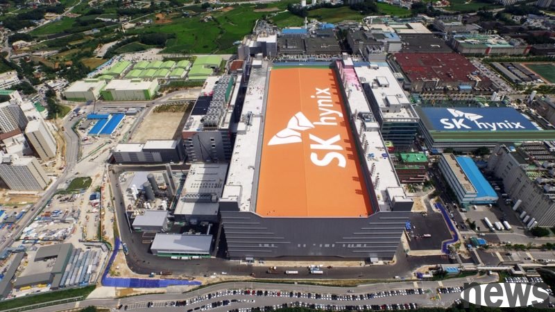
Korean memory factory SK Hynix announced on the 3rd that it has introduced the first mass-produced high-number hole ultraviolet exposure machine (High NA EUV) in the memory industry to the M16 factory in Lichuan, South Korea, and held a equipment entry ceremony.
SK Hynix said that high-numeric pore ultraviolet exposure machines have higher numeric pores than the current standard EUV, because numeric pores are used to measure the ability of lens-transmitting light concentrating. Therefore, the larger the numerical hole, the higher the precision of the circuit pattern drawing. The resolution can be further greatly improved, and the process of drawing the most detailed circuit pattern at present is expected to play a key role in reducing the width of the line and improving integration.
Equipment entry ceremony, ASML Korean President Jin Bing-chan, SK Hynix Future Technology Officer and Chief Technology Officer (CTO) Car Xuanlong, SK Hynix Manufacturing Technology Executive Li Bingqi and other leaders attended the ceremony, wishing the introduction of the next generation of DRAM production equipment.
SK Hynix pointed out that the global semiconductor market competition is becoming increasingly fierce, and it has successfully established a practical foundation for rapid research and development and supplying high-end products to meet customer needs. Close cooperation with partners to enhance the reliability and stability of global semiconductor supply chains. At present, in order to improve product performance and production efficiency, microprocessor optimization is particularly important. The more precise the circuit pattern is, the more wafers each circle can produce, and it also effectively improves energy efficiency and performance.
SK Hynix has been introduced into EUV technology for the first time in 2021 in the fourth generation of 10-nanometer (1a) DRAM, and has continued to expand EUV applications to advanced DRAM manufacturing. However, in order to meet the future demand for ultra-finement and high integration in the semiconductor market, it is essential to introduce next-generation technical equipment beyond existing EUVs. Therefore, the equipment introduced this time is TWINSCAN EXE:5200B launched by ASML in Dutch. It is the first mass-produced High-NA EUV device. Compared with the existing EUV device (NA 0.33), the optical performance (NA 0.55) is improved by 40%, and the precision of the circuit pattern can be produced up to 1.7 times, and the integration degree is increased by 2.9 times.
SK Hynix has emphasized that it will simplify EUV technology in new equipment, accelerate the research and development of next-generation memory, ensure product performance and cost competitiveness, and is expected to consolidate the position of the high-value-added memory market and strengthen technical leadership.