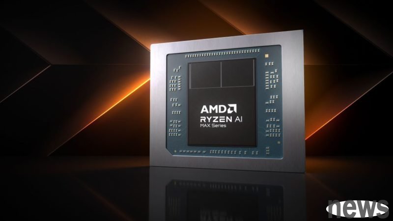
Market news pointed out that the processor manufacturer AMD's next-generation Zen 7 architecture processor is run on an AM5 interface, which means that AM5 interface motherboard users can use the next-generation 32C/64T Zen 7-based Ryzen CPU.
As early as December 2023, AMD promised that the AM5 interface will continue to be used until 2025 and beyond, and will be used on the next generation of Zen 6 architecture processors, including Zen 3, Zen 4 and the current generation of Zen 5, and the next generation of Zen 6 architecture processors expected to be released in 2026. As for the next Zen 7 architecture processor, it is expected to be released in 2028. The latest market news points out that AMD has decided to still be running on the AM5 interface.
If market news is true, the Zen 7 architecture will be built on the AM5 interface, which will be one of the longest CPU interface support versions we have seen, similar to the recent Intel next-generation LGA 1954 interface that supports at least third and fourth generation Intel CPUs, but the AM5 interface has been introduced, and anyone based on the Zen 3 architecture processor can upgrade to Zen 5, Zen 6, or even to Zen 7.
This represents the AM5 interface that supports 32 Ghorda cores and 64 execution products. Zen 7 processors have 16 cores per chip and 32 cores a double chip. Later, the older AM5 interface motherboard for 32C/64T processors is a better choice because it will make the AM5 interface longer.
AMD's next-generation Zen 6 architecture Olympic Ridge CPU will be equipped with an improved I/O chip to support higher RAM speeds. This is another major upgrade, which means that Zen 5 will no longer use the same I/O chip as the Zen 4 interface. The Zen 7 architecture has higher I/O chips than the Zen 6 architecture, and the AM5 interface motherboard has been upgraded to Zen 7 with more advantages, such as more cores, higher-temporal, improved I/O chips, etc.
Zen 7 architecture contains three cores, one is a high-performance density core, a new low-power core that implements maximum input and output construction and performs capabilities tasks, similar to the Intel LP/E core. There is also an unspecified PT and 3D core. Changing the operating module and adjusting the module, AMD can differentiate each core to achieve optimal performance, such as cloud-enabled virtual machine-to-network AI processing.
In terms of manufacturing, the computing chip (CCD) of the Zen 7 architecture processor adopts the A14 process of power supply network, including the back side power supply network. The 3D V-Cache SRAM below the wafer retains the tyrene N4 process, which is a conservative choice. Telco talks about the use of N2 process-based chip stacking memory for high-level packaging, but AMD is very cautious about this and the cache size should also increase. Each core will receive 2MB of L2 cache, and each core L3 cache can be expanded to 7MB through stacked V-Cache slices, so that there are still about 32MB of shared L3 without V-Cache.
Overall, there are at least four versions of the Zen 7 architecture, including the classic Zen 7 that focuses on high performance, the intensive Zen 7c of high-core number server solutions, the low-power Zen 7 that prioritizes power consumption and chip surfaces, and the efficient Zen 7 with efficiency and IPC goals. But that's not all, AMD seems to be able to pack up to 33 cores per computing chip, and the flagship server EPYC CPU can accommodate a total of 264 cores. The Zen 5c architecture has only 192 cores at most.